Study of exciton and spin/valley dynamics in two-dimensional semiconductors and their heterostructures
The discovery of graphene (2004) has revolutionised the scientific landscape due to its unique optical and electronic properties deriving from its peculiar band structure. Today, many other materials exhibiting a wide range of chemical structure and electronic properties have been isolated in two-dimensional mono- or few-layer form.
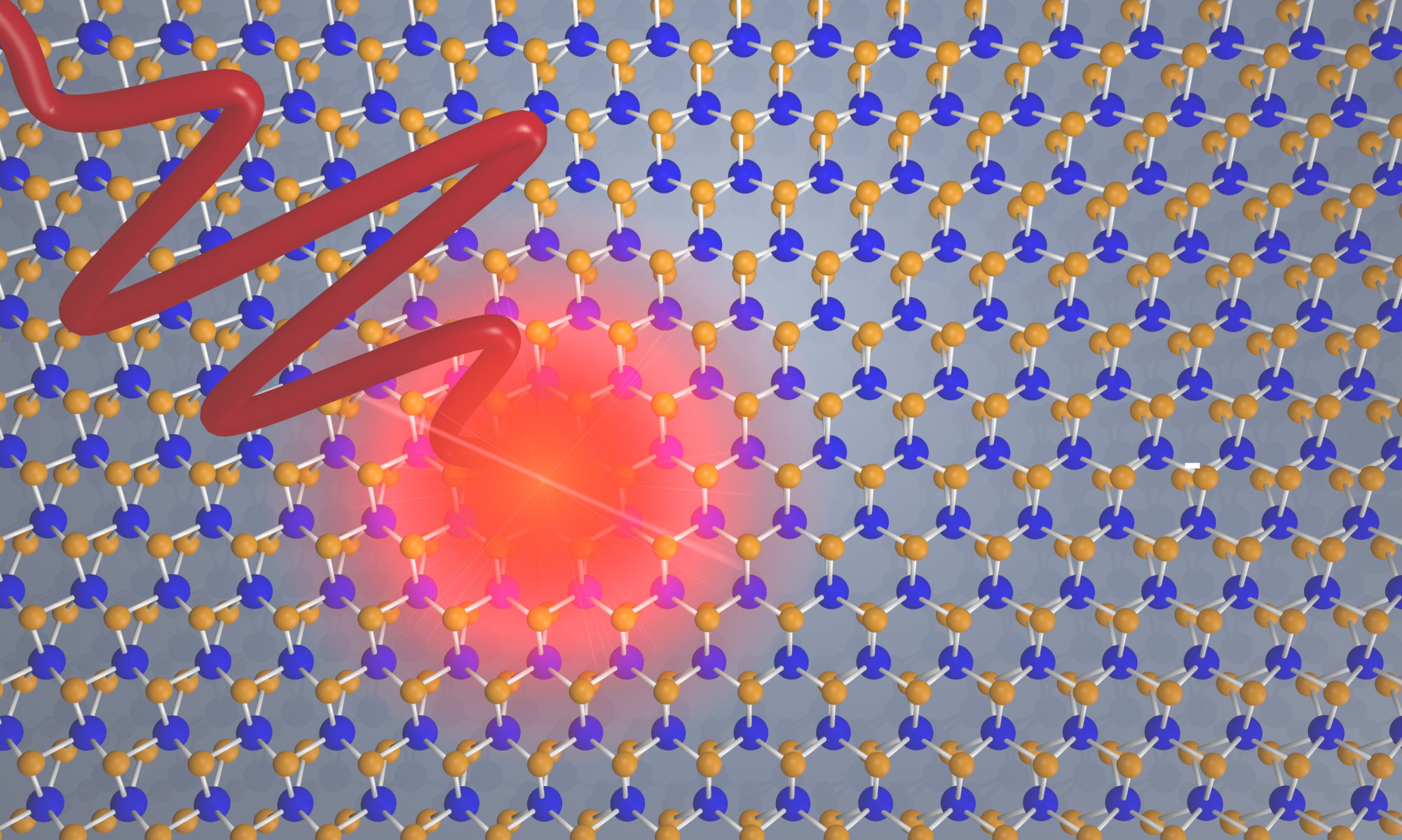
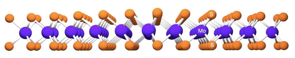
Within the 2D materials, a particular interesting family are the Transition Metal Dichalcogenides (TMD). A single sheet of TMD is formed by a hexangular lattice of transition metal atoms (M) sandwiched between to hexagonal lattices of chalcogen atoms (X). Among the possible combinations, the best studied TMD compounds are those with M=Mo or W, and X=S or Se. (MoS2, MoSe2, WS2 and WSe2).
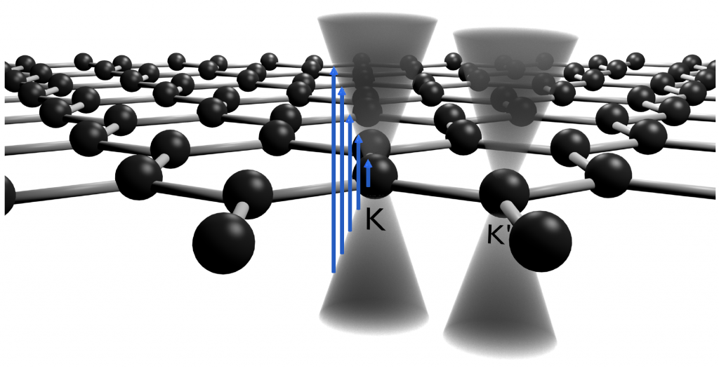
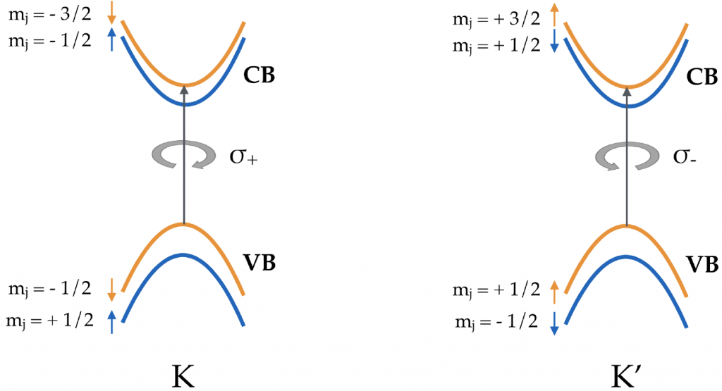
Contrary to the semimetallic graphene, these TMDs are semiconductors and bear a large potential for a new generation of electronic and optoelectronic devices. They drastically change their band structure from indirect to direct gap upon thinning them to monolayers. The monolayer band structure exhibits two non-equivalent valleys at the K and K’ points at the edge of the Brillouin zone. Strong spin-orbit interaction and inversion symmetry breaking makes the valence and conduction bands spin-polarized at K and K’. Therefore, using circularly polarized light, we can selectively populate one of the valleys with spin-polarized carriers. The possibility to use this degree of freedom for quantum computation has initiated the field of “valleytronics”.
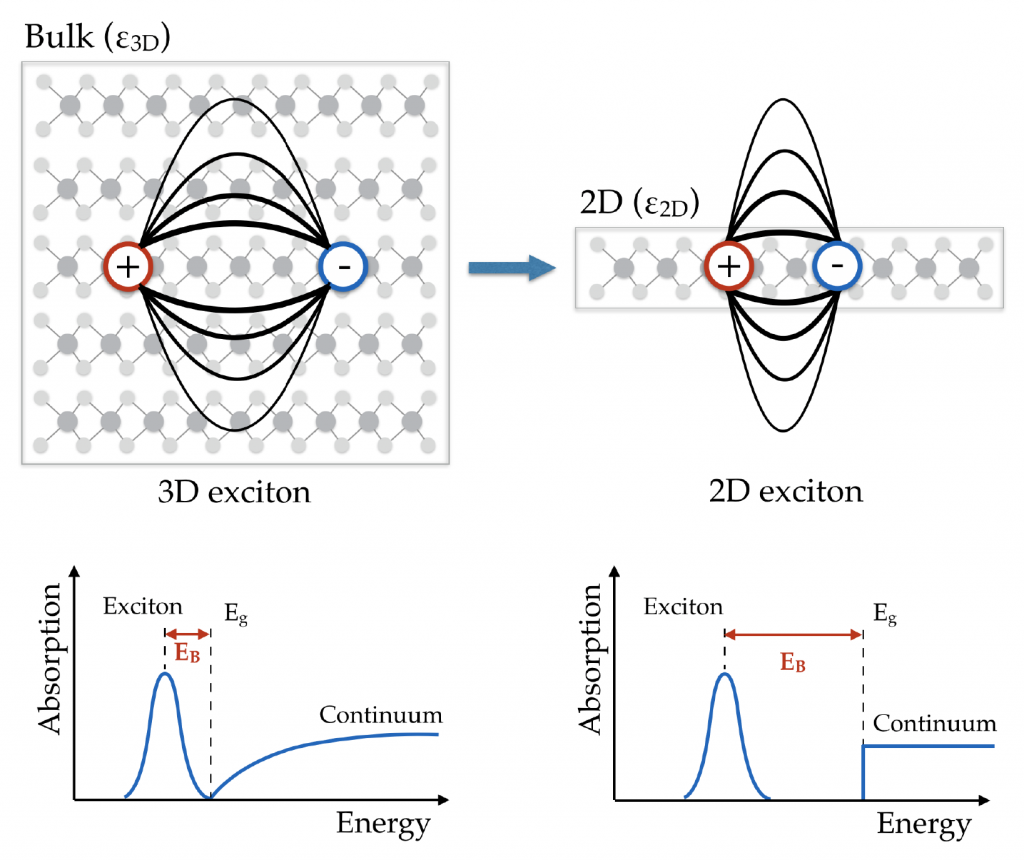
Another important property of TMDs is that due to the strong quantum confinement the Coulomb interaction between the electrons and holes is only weakly screened. Therefore, the binding energy of excitons (bound states of one electron and one hole) is several hundred meV, almost two orders of magnitude higher than in semiconductor quantum wells. Their optical properties are dominated by excitonic effects also at room temperature. Despite the ample body of experimental results and modelling, their non-equilibrium optical properties, which determine their functionalities for devices, are not yet fully understood and are the object of ongoing investigation [1].
Experimental works are focussed on:
– Studying the dynamics of photogenerated charges and excitons in semiconducting TMD using optical pump/probe spectroscopy [2,3]. The candidate will use the pump-probe microscopy set-up realised in the “Clark” ultrafast spectroscopy lab to study the relaxation, recombination and bandgap renormalisation [4] mechanisms that dominate TMDs’ non-equilibrium response.
Partners: Cambridge Graphene Center, ICFO, Technical University of Wien, CNR-ISM, Columbia University (New York).
– Study of the spin/valley dynamics in semiconducting TMDs via time-resolved Farady/Kerr rotation and circular dichroism experiments. The candidate will use the pump-probe microscopy set-up realised in the “Clark” ultrafast spectroscopy lab and the more recent set-up in the “Ultras” lab to study inter- and intraband scattering processes for different temperatures and doping levels [4,5].
Partners: Cambridge Graphene Center, ICFO, Technical University of Wien, CNR-ISM, Columbia University (New York).
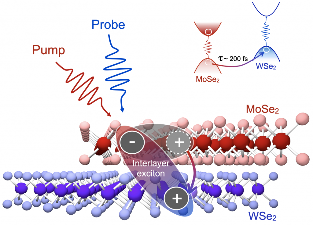
– Study of the charge transfer dynamics in TMD heterobilayers and mixed TMD-graphene heterostructures. This process enables 2D materials based photovoltaics. The transfer mechanism and its dependence on the twist angle between the individual layers is still largely unknown. Preliminary results show also the possibility to maintain the valley polarisation during the charge transfer and create long-lived valley polarized carrier populations. The candidate will use the pump-probe microscopy set-up realised in the “Clark” ultrafast spectroscopy lab and the more recent set-up in the “Ultras” lab to study the charge and valley polarisation transfer process for different temperatures [6] and twist angles.
Partners: Cambridge Graphene Center, ICFO, University of Texas, IIT (Pisa), Columbia University (New York), University of Southern California.
Bibliography
[1] S. Dal Conte et al. Trend in Chemistry (2019) article in press (https://doi.org/10.1016/j.trechm.2019.07.007)
[2] C. Trovatello et al. Nature Communications 11, 5277 (2020)
[3] C. Trovatello et al. ACS Nano 14, 5, 5700-5710 (2020)
[4] E. A. A. Pogna et al. ACS Nano 10, 1182-1188 (2016)
[5] S. Dal Conte et al. Phys. Rev. B 92, 235425 (2015)
[6] Z. Wang et al. Nano Lett. 18, 11, 6882-6891 (2018)
Contacts
Prof. Giulio Cerullo, giulio.cerullo@polimi.it
Dr. Stefano Dal Conte, stefano.dalconte@polimi.it
Prof. Christoph Gadermaier, christoph.gadermaier@polimi.it